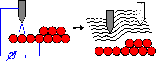
The Scanning Tunneling Microscope (STM) was introduced by G. Binnig and W. Rohrer at the IBM Research Laboratory in 1982 which was honoured by the Noble Prize in 1986. It has become widely used as an important instrument for real space analysis in surface science.
The basic idea is to bring a fine metalic tip in close proximity
(a few Å) to a conductive sample. By applying a voltage (U![]() 4V) between
the tip and the sample a small electric current
(0.01nA-50nA) can flow from the sample to the tip or reverse, although the
tip is not in physical contact with the sample. This phenomenon is called
electron tunneling . The
exponential dependence of the tunneling
current on the tip to sample distance results in a high vertical resolution. By
scanning the
tip across the surface and detecting the current (one can also use the
current as a vertical positioning signal for the tip - see
Modes of Operation ) a map of the surface can be generated with a resolution in the order of
atomic distances. It has to be mentioned that the image cannot just be interpreted as a
topographic map as the tunneling current is influenced by the lateral and vertical
variation of the electronic state density at the surface.
The lateral resolution is about 1Å whereas a vertical resolution
up to 0.01Å can be achieved.
The STM can be used in ultra high vacuum, air or other environments.
4V) between
the tip and the sample a small electric current
(0.01nA-50nA) can flow from the sample to the tip or reverse, although the
tip is not in physical contact with the sample. This phenomenon is called
electron tunneling . The
exponential dependence of the tunneling
current on the tip to sample distance results in a high vertical resolution. By
scanning the
tip across the surface and detecting the current (one can also use the
current as a vertical positioning signal for the tip - see
Modes of Operation ) a map of the surface can be generated with a resolution in the order of
atomic distances. It has to be mentioned that the image cannot just be interpreted as a
topographic map as the tunneling current is influenced by the lateral and vertical
variation of the electronic state density at the surface.
The lateral resolution is about 1Å whereas a vertical resolution
up to 0.01Å can be achieved.
The STM can be used in ultra high vacuum, air or other environments.
