5. Examples

Determination of surface structures is one of the most important applications of the STM. It is obvious that a lot of surfaces reconstruct to lower their energy. Thus the properties of the surfaces can be completely different from the bulk. Especially due to the size reduction in semiconductor technology surface properties are getting important. A few examples of surface science studies are given below, all illustrated using STM images taken at the Erlangen surface lab.

5.1. Si(111)7x7

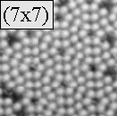
Si 7x7
Si 7X7
The imaging of the Si(111)- 7x7 was the first great success of the STM although the structure could not be resolved completely. This has been later achieved with the help of high resolution transmission electron microscopy. Before the invention of STM it was known from LEED experiments that the surface unit cell is constructed of 49 Si(111) original cells. It was also assumed that the cell has a sixfold symmetry.
STM images show that there are 12 adatoms in each unit cell. Further, in each corner of the cell a hole exists (corner hole). Using the proper tunneling voltage (about -0,35V) it can be seen that the cell consists of two different triangles and thus infact has a threefold symmetry.
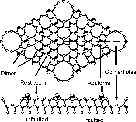
A complete description of the stucture is given by the DAS model (Dimer Adatom Stacking fault) (after Takaynagi et al., 1985.)
DAS Model
DAS Model
Its features are:

5.2.Au(111)22x


When the first Au(111) STM images with atomic resolution were taken some features had already been known or assumed by LEED experiments and helium scattering experiments:
Au(111)
Atomic resolution of Au(111)
STM images reveal the following results:
  • At low resolutions the two ridges can be detected
  • With atomic resolution the atoms can be seen gradual displaced along the [10] direction are (maximum displacement: 0.7Å)
  • In larger areas the stripe can appear in three directions 120 apart
  • In regions where the atoms are raised due to their dislocation the corrugation is larger
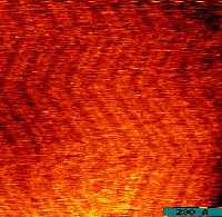
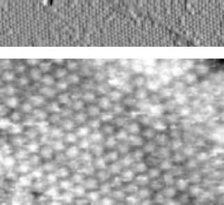
But beside the confirmation of the proposed model of Au(111) reconstruction STM experiments give also information about aperiodic structures, which diffraction experiments are insensitive to. As gold exhibits a threefold symmetry, the three directions which the ridge can run along are of equal probability. Thus between regions with different reconstruction, domain boundaries are formed. On large areas the double ridges change orientation about every 280Å. This leads to the so called herringbone structure. On an even larger scale herringbone structures of different orientation form a mosaic structure. It has also become evident that the herringbone structure is quite sensitive to defects like e.g. step edges. Au(111)
Herringbone structure of Au(111)

5.3. SiC(0001) 3x3

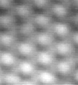
With a large band gap, a high break down field and a high saturation drift velocity of the conducting electrons SiC is an interesting material for semiconductor technology. Thus its surface strucure and the surface electronic properties are of a great importance for material growth and device fabrication. SiC surface show a variety of surface reconstructions. One of those structures is the (3x3) phase on SiC(0001) whose actual atomic geometry has long been unresolved.
STM experiments provided some insight in the structure:
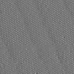
  • there is a single protrusion per unit cell
  • the corrugation is independant of the tunneling voltage
  • large cornerholes can not be seen
SiC
3x3 4H SiC (0001)

SiC(0001)3x3


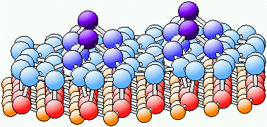
Combining this with results from electron spectroscopy and low-energy electron diffraction (LEED) The surface geometry could be determined in detail.
SiC Model
SiC(0001) 3x3 Model
The properties of the SiC(0001) 3x3 structure are:
  • a compact, planar Si adlayer with sp2 hybridisation within the layer,
  • a twist rotation of the Si-trimer covering the adlayer and its surrounding atoms within the adlayer,
  • single dangling bond per (3x3) unit cell located at the adatom ontop of the trimer,
  • ideal Si-Si bond lengths (2.31-2.39Å) and fourfold coordination of all other atoms.


previous next